CS 4141 — Digital Systems Laboratory, Lab 4 — Pre-Lab
Learn about D Flip-Flop IC 7474. Draw truth table for the output Q and Q’. Consider all inputs including Clock, CLEAR (Reset), PRESET and data pin D.
| CLK | CLEAR | PRESET | D | Q | Q’ |
|---|---|---|---|---|---|
| X | 1 | 0 | X | 1 | 0 |
| X | 0 | 1 | X | 0 | 1 |
| X | 0 | 0 | X | H↑ | H↑ |
| ↑ | 1 | 1 | 1 | 1 | 0 |
| ↑ | 1 | 1 | 0 | 0 | 1 |
| 0 | 1 | 1 | X | Q0 | Q’0 |
Learn about JK Flip-Flop IC 74107. Draw truth table for the output Q and Q’. Consider all inputs including Clock, Clear, data pin J, and data pin K.
| CLEAR | CLK | J | K | Q | Q’ |
|---|---|---|---|---|---|
| 0 | X | X | X | 0 | 1 |
| 1 | ↓ | 0 | 0 | Q(prev) | Q’(prev) |
| 1 | ↓ | 1 | 0 | 1 | 0 |
| 1 | ↓ | 0 | 1 | 0 | 1 |
| 1 | ↓ | 1 | 1 | 1 | 0 |
| 1 | 1 | X | X | Q(prev) | Q’(prev) |
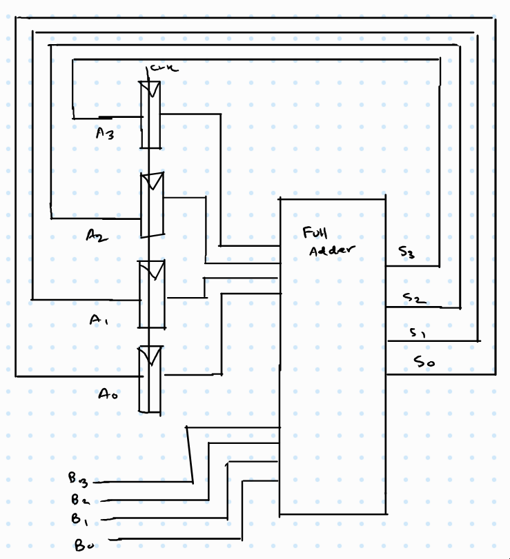
This problem involves building a tiny ALU performing 4-bit addition and using two 74SL74 (4 DFF’s) and a 4-bit adder. Provide an implementation to perform the following ALU addition operation. Add A,B – This operation adds register A and input B and stores the result in register A. Create a 4-bit register using 4 D FFs which acts as an accumulator. This accumulator is connected with an adder and is performing the following task. The initial value of the accumulator is 0 and every time a clock pulse is given, it adds the current value of the accumulator (let’s call it A) and a given 4-bit input B. The B input is provided using 4 input switches. Thus, the accumulator stores the addition of multiple 4-bit values provided to the ALU. Draw the Logic Diagram of a tiny ALU with DFF Accumulator. Use logical symbols, not IC chips. A logical diagram should contain block notations (such as Full Adder, D Flip-Flop, Decoder, Multiplexer) and gate symbols (such as AND, OR, and NOT).